About
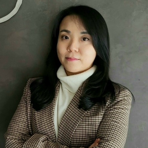
I am a Ph.D. candidate in Electrical and Computer Engineering at the Georgia Institute of Technology, advised by Dr. Shimeng Yu in the Laboratory for Emerging Devices and Circuits, and an SRC Research Scholar (SPARC). My thesis is Next-Generation 3D Scaling: Reliability-Aware Device-to-System Co-Optimization for Advanced CMOS Logic and Memory.
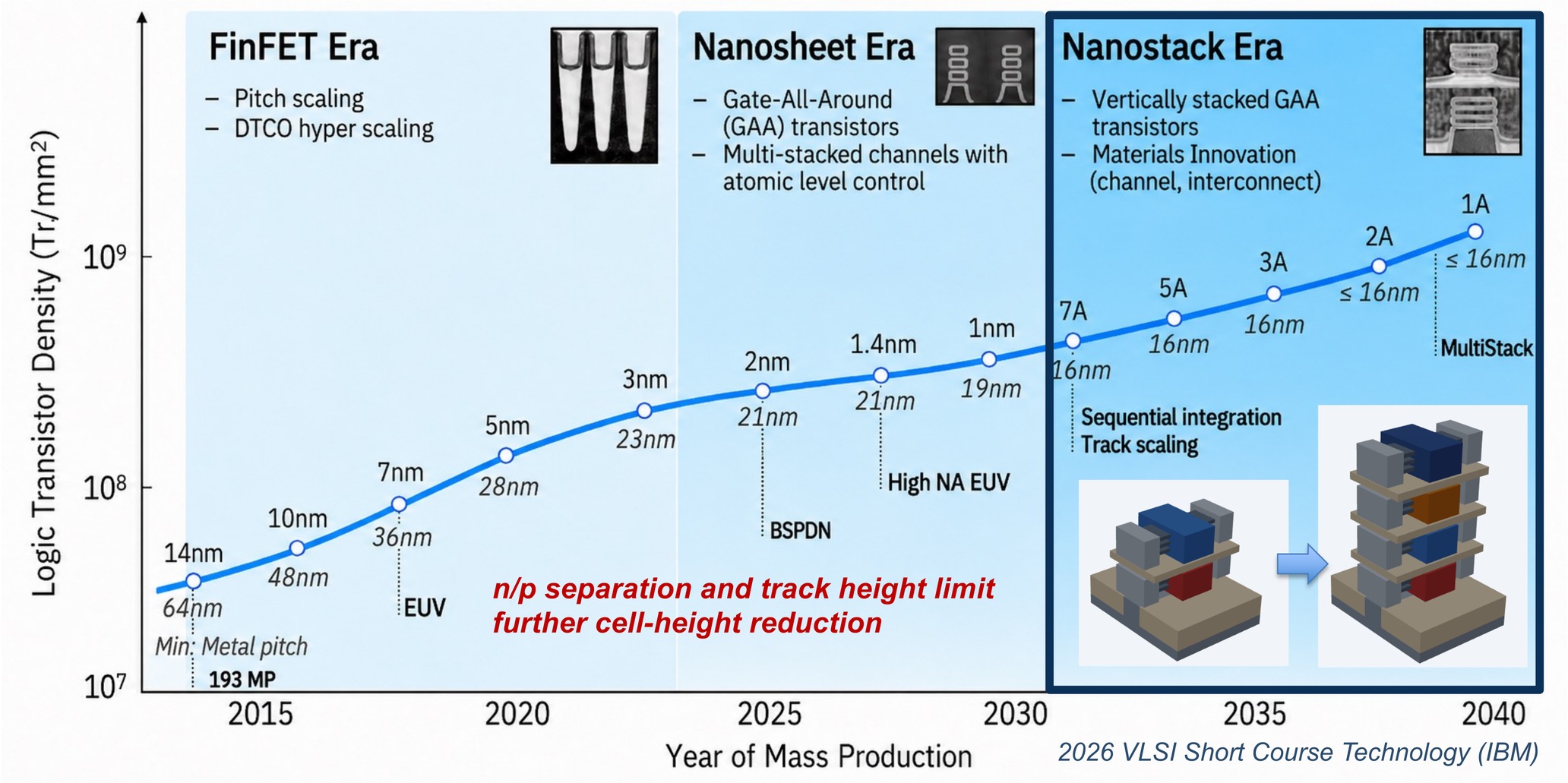
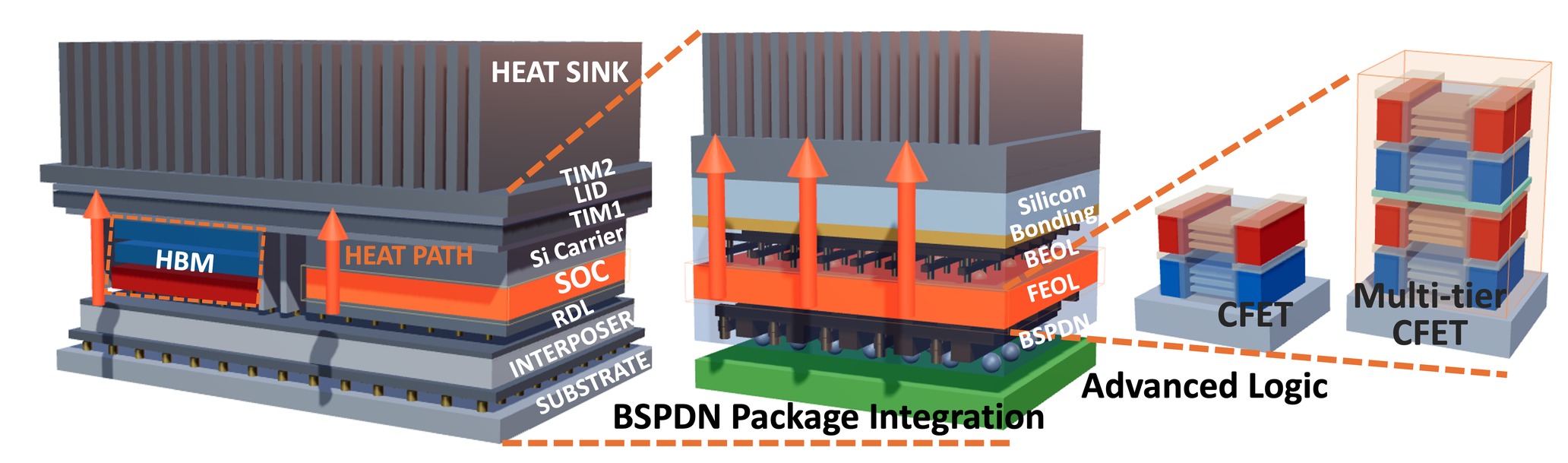
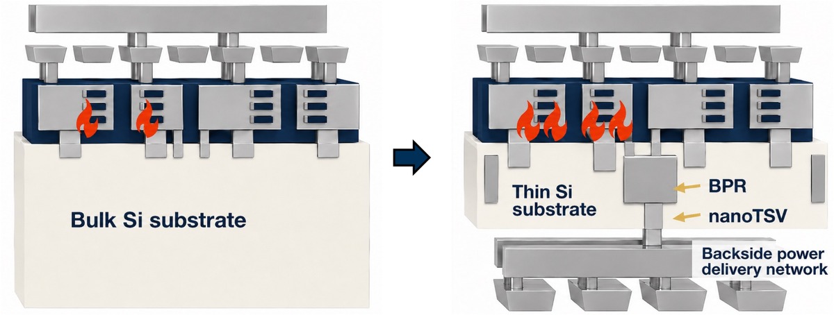
Before graduate school I spent seven years at Samsung Electronics as a Technology Quality & Reliability engineer, building the aging-aware design environments, reliability models, and sign-off methodologies behind Exynos SoCs from 14 nm through 4 nm and 3 nm GAA nanosheet technology. That industry background is what shapes my research question: once devices stack and power delivery moves to the backside, heat has a longer path out of the die and reliability margins tighten, so self-heating and aging have to be budgeted up front, the way timing and power already are.
I am currently a Design Quality & Reliability Engineer Intern at Intel in Hillsboro, OR, developing physics-informed machine learning methods for pre-silicon reliability of analog IP and memory circuits, targeting CPU, server, and ASIC products.
Research
3D Compute-in-Memory
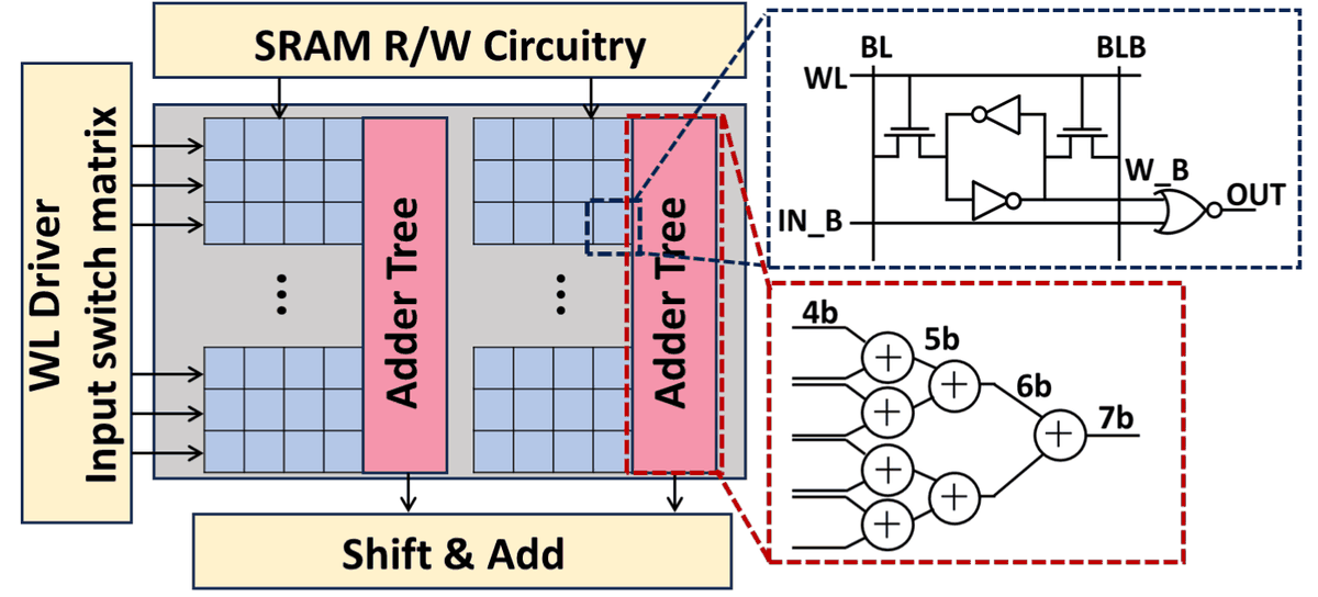
Digital compute-in-memory benchmarking on A5 CFET technology, extended to look-up-table-based power efficient design, targeting the memory wall across the memory pyramid. [L4]
| Capability | ASAP7 | ASAP5 | FreePDK3 | GT3 | USC 3N-2D | MATRIX-A5(this work) |
|---|---|---|---|---|---|---|
| Institution | ASU | ASU | NCSU | Georgia Tech | USC (SCCAD) | Georgia Tech |
| Node | 7 nm | 5 nm | 3 nm | 3 nm | 3 nm | A5 |
| Device | FinFET | NWFET | GAA NS | GAA NS | GAA NS | CFET |
| Integration | 2D | 2D | 2D | 2D | 2D | 3D stacked device |
| Standard-cell library | ✓ | ✓ | ✗ | ✓ | ✓ | ✓ |
| Multi-Vth flavors | ✓ | ✗ | ✗ | ✗ | ✗ | ✓ |
| Temperature corners | ✓ | ✗ | ✗ | ✗ | ✗ | ✓ |
| RTL-to-GDS flow | ✓ | ✓ | ✓ | ✓ | ✓ | ✓ |
| Backside power (BSPDN) | ✗ | ✗ | ✗ | ✓ | ✓ | ✓ |
| Availability | open | open | open | open | open | will be open |
Experience
Design Quality & Reliability Engineer Intern
Aug 2026 – Jan 2027
- Product Quality Network team: developing physics-informed machine learning methods for pre-silicon reliability of analog IP and memory circuits, targeting CPU, server, and ASIC products.
Graduate Research Assistant
Aug 2023 – Present
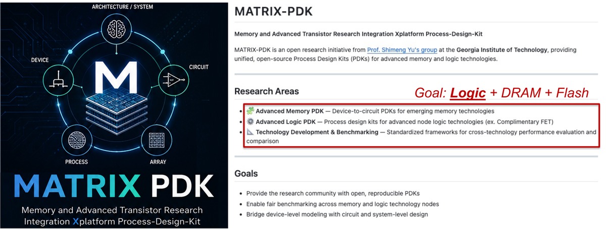
- Open-source CFET PDK and multi-tier DTCO/STCO — TCAD-calibrated device models and the first open-source sequential-CFET PDK (six 67-cell library variants) taken through a complete RTL-to-GDSII flow; 40% logic and 43% SRAM cell-footprint reduction from 2-tier to 4-tier. [L1, L2, L3]
- Block-level technology benchmark — a RISC-V core and a 16×16 systolic array through synthesis, place-and-route, and timing and power analysis: CFET cut standard-cell area 27.5% against a GAA-nanosheet baseline for a 14.5% power cost at iso-frequency, and a hybrid-row track-mixing scheme (CFlex) closed a 1.5 ns clock that a dense-only library could not meet. [L1]
- Reliability-aware co-optimization — device-to-circuit electro-thermal framework (TCAD to self-heating-aware compact model to ring-oscillator analysis) showing that backside power delivery traps heat: over 10% ring-oscillator frequency degradation at 1.3 V, against under 5% with frontside delivery; GPU-accelerated multi-physics (DeepSim) extended to multi-tier CFET for layout-resolved analysis. [R1, R2]
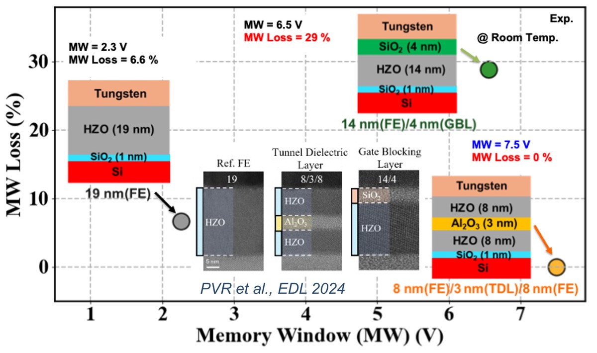
- Memory devices and in-memory compute — CFET digital compute-in-memory (DCIM) against the memory wall, and ferroelectric gate-stack and channel-side interlayer modeling in FeFET and Fe-NAND, where a gate-injection-layer stack more than doubles the memory window. [L4, F1, F3, F4]
Technology Quality & Reliability Engineer
Aug 2016 – Jul 2023
- Delivered aging- and variability-aware design methodologies for Samsung Exynos SoCs (14 nm – 4 nm) under advanced reliability sign-off.
- Developed statistical aging simulation modeling and methodology, enabling AEC-Q100 automotive-grade design-for-reliability in 8 nm FinFET products.
- Partnered with Design Technology Enablement to deliver critical-path reliability timing margin from aging simulation directly into the Exynos SoC implementation flow.
- Built aging-aware circuit design environments and PDK components for 3 nm GAA nanosheet technology.
- Built and validated reliability models for HCI, BTI, TDDB, and self-heating, improving prediction accuracy through model-to-hardware correlation against ring-oscillator silicon benchmarks with the WLR and PDK teams.
- Provided DFR for real product operating conditions (multi-step aging, power-down bias instability) rather than idealized stress, closing the gap between qualification and field use.
- Verified overdrive-voltage reliability in non-volatile memory (eFuse, OTP, MRAM) under product stress conditions.
- Prior internship (Jul – Aug 2016): implemented enhanced Dynamic Device Voltage Check (DDVC); strengthened safe-operating-area (SOA) validation and voltage-stress reliability sign-off across advanced nodes.
Education
Georgia Institute of Technology
Ph.D., Electrical and Computer Engineering · Atlanta, GA
Sogang University
B.S., Electronic Engineering · Seoul, South Korea · summa cum laude
University of Connecticut
International Student Exchange, Electrical and Computer Engineering · Storrs, CT
Technical Skills
- Focus
- Reliability- and thermal-aware DTCO/STCO; multi-tier CFET and 3D integration; physical design and timing closure; ferroelectric device modeling; aging and reliability sign-off.
- Reliability physics & sign-off
- HCI, BTI, TDDB, self-heating, SOA; statistical aging simulation; model-to-hardware correlation; AEC-Q100 automotive qualification.
- TCAD & device
- Sentaurus electro-thermal device/process; BSIM-CMG compact modeling.
- VLSI design & implementation
- Synopsys Design Compiler; Cadence Innovus (place-and-route, floorplan, CTS, congestion and timing closure); static timing analysis (Cadence Tempus); power analysis; parasitic extraction (Quantus, StarRC); custom cell layout (Cadence Virtuoso); full PDK build and verification (LIB/LEF, LPE, DRC/LVS); reliability sign-off and critical-path timing-margin analysis.
- Circuit simulation
- SPICE (HSPICE, FineSim, Spectre) with aging engines (RelXpert, MOSRA); Dynamic Device Voltage Check (DDVC); multi-step and power-down-bias stress modeling.
- Technologies
- FinFET, GAA nanosheet, multi-tier CFET, backside power delivery, ferroelectric-based memory.
- Programming
- Python, TCL, Perl, C, MATLAB, SystemVerilog.
Honors & Awards
- Best Paper Award, Runner-Up — IEEE Device Research Conference (DRC) Jun 2025
- Silicon Creations ISSCC Travel Grant Feb 2024
- Conference Travel Grants — APCCAS'24, IRPS'25, DRC'25, IEDM'25 (presentation) 2024 – 2025
- CSE Department Fellowship (offered) — University of Minnesota–Twin Cities Jan 2023
- Summa cum laude — Sogang University; Dean's List Aug 2016
- Full National Scholarship (Merit) — Korea Student Aid Foundation 2014 – 2016
- Honors Scholarship (Merit) — Sogang University 2012 – 2015
Leadership & Service
- Ministry Team Leader, Grad CRU — Georgia Institute of Technology 2024 – Present
- Education Mentor / Sub-Course Manager — Samsung Electronics 2019, 2020, 2022 Delivered onboarding for 200+ new hires: "Global Business Manners," "Communication & Creative Thinking."