Selected work, grouped by topic

Publications

Twelve entries across 3D logic and SRAM DTCO/STCO, ferroelectric devices and memory reliability, and reliability and electro-thermal co-design. Bold names indicate my authorship; * denotes equal contribution.

3D Logic & SRAM DTCO/STCO 4 entries

MATRIX-PDK identity graphic: device, circuit, array, process and architecture icons arranged around a stacked-die symbol
[L1]
MATRIX-A5: An Open-Source CFET PDK with CFlex Track-Mixing Libraries for RTL-to-GDSII DTCO
Shon, M.*, Lim, S.*, et al., Yu, S.
IEEE Journal on Exploratory Solid-State Computational Devices and Circuits (JXCDC), 2026
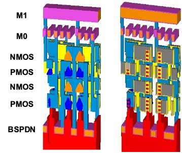
Two three-dimensional standard-cell renders showing the M1 and M0 metal levels above stacked NMOS, PMOS, NMOS and PMOS device tiers over a backside power delivery network
[L2]
DTCO of Multi-Tier CFETs: Ultimate Logic and SRAM Scaling of A5 Technology and Beyond
Shon, M.*, Lim, S.*, Yu, S.
IEEE International Electron Devices Meeting (IEDM), 2025
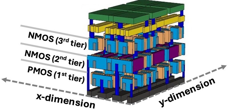
Three-dimensional render of a 3-tier CFET SRAM cell, labelled with a PMOS first tier, an NMOS second tier and an NMOS third tier, with x-dimension and y-dimension arrows along the base
[L3]
3-Tier SRAM Complementary FET (CFET) High Density (HD) Cell Design at A5 Node
Lim, S., Shon, M., Yu, S.
IEEE Transactions on Electron Devices (TED), 2025
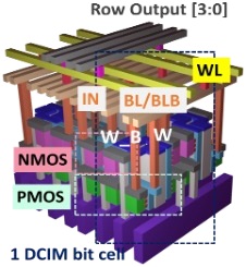
Three-dimensional render of one digital compute-in-memory bit cell with word line, input, bit line and bit line bar routing above stacked NMOS and PMOS tiers, feeding a four-bit row output
[L4]
3D Digital Compute-in-Memory Benchmark with A5 CFET Technology: An Extension to Look-up-Table Based Design
Lee, J.*, Shon, M.*, et al., Yu, S.
IEEE Transactions on VLSI Systems (TVLSI), 2025

Reliability & Electro-Thermal Co-Design 3 entries
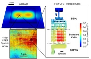
Package-level thermal map with two hotspots, a thermal micrograph of a 4-tier CFET systolic array, and a cross-section of 4-tier CFET hotspot cells from BEOL through the standard cells to the backside power delivery network, coloured by temperature rise from 51 to 57 degrees Celsius
[R1]
AI-Accelerated, Layout-Resolved Electro-Thermal Analysis for Multi-Tier CFET LogicSubmitted
Shon, M.*, McClellan, C. J.*, et al., Yu, S.
IEEE International Reliability Physics Symposium (IRPS), 2027
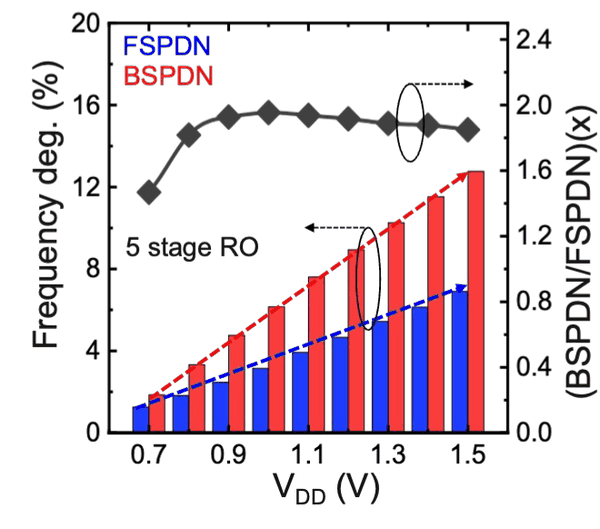
Frequency degradation against supply voltage for a five-stage ring oscillator with frontside and with backside power delivery, rising from about 1 percent at 0.7 volts to roughly 7 percent frontside and 13 percent backside at 1.5 volts, with the backside to frontside ratio holding near 1.9 across the range
[R2]
Self-Heating in GAA Nanosheet FETs with Integrated Back Side Power Delivery Network: Device to Circuit Electro-Thermal Analysis and Implications
Dutta, R.*, Shon, M.*, et al., Datta, S.
IEEE International Reliability Physics Symposium (IRPS), 2026

Samsung Electronics
[R3]
Aging-Aware Design Verification Methods Under Real Product Operating Conditions
Shim, H., Jo, J., Kim, Y., Jeong, B., Shon, M., et al., Pae, S.
IEEE International Reliability Physics Symposium (IRPS), 2019

Ferroelectric Device & Memory Reliability 4 entries
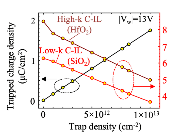
Trapped charge density against trap density for a high-k channel-side interlayer of hafnium oxide and a low-k interlayer of silicon dioxide at a write voltage magnitude of 13 volts
[F1]
Channel-Side Interlayer Engineering in Laminated FeFETs: Trap-Driven Optimization of Memory Window, Retention, and Disturb in Ferroelectric NAND Flash
Fernandes, L.*, Shon, M.*, et al., Khan, A.
IEEE International Reliability Physics Symposium (IRPS), 2026
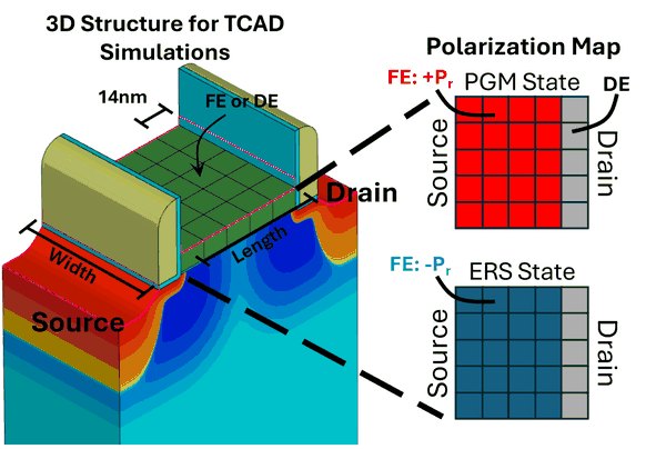
Three-dimensional FeFET structure used for TCAD simulation with a 14 nm ferroelectric or dielectric gate region, beside polarization maps of the programmed and erased states across the channel from source to drain
[F2]
On the Localized Ferroelectric Phase Variation in Scaled FeFET: Experiments and Modeling
Phadke, O., Shon, M., et al., Yu, S.
IEEE International Electron Devices Meeting (IEDM), 2025
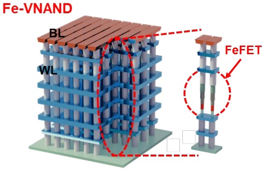
Three-dimensional ferroelectric vertical NAND array with bit lines and word lines, and a detail of the FeFET cell within the vertical string
[F3]
Modeling Dynamic Interplay Between Charge Traps and Polarization for Memory Window Enhancement in Gate Injection Layers
Shon, M., et al., Yu, S.
IEEE International Reliability Physics Symposium (IRPS), 2025
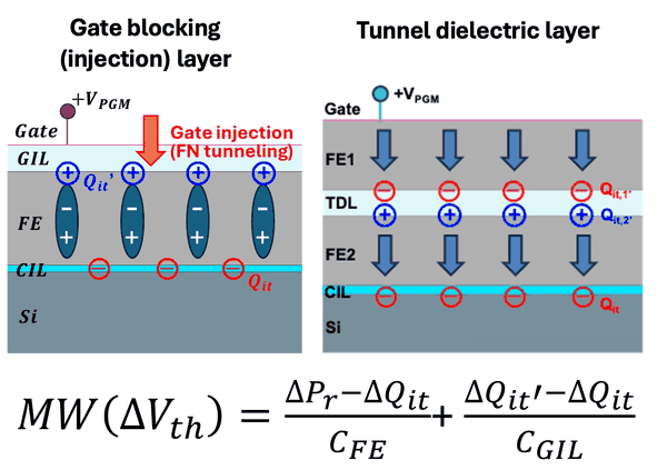
Band schematics of a gate blocking injection layer with Fowler-Nordheim gate injection and of a tunnel dielectric layer between two ferroelectric films, with the memory window expression in terms of remanent polarization, interface trapped charge, and ferroelectric and gate-injection-layer capacitance
[F4]
A Comprehensive Modeling of Gate Stack Interlayer Engineering for Ferroelectric Vertical NAND
Shon, M., et al., Yu, S.
IEEE Device Research Conference (DRC), 2025 · Best Paper Award, Runner-Up

Tutorial Presentation 1 entry

MATRIX-PDK identity graphic: device, circuit, array, process and architecture icons arranged around a stacked-die symbol
[T1]
MATRIX Open-Source PDKs for Advanced DRAM and Sub-1-nm CFET Logic: From Device Models to RTL-to-GDSII Design-Technology Co-Optimization
Presenters: Yu, S., Shon, M.
Asia and South Pacific Design Automation Conference (ASP-DAC), 2027

Five of these appeared at IEEE IRPS (2019, 2025, 2026 ×2, 2027).